
Wellness
How to Establish Healthy Digital Boundaries Post-Work for Better Work-Life Balance

For decades, the focus of semiconductor innovation has centered on shrinking the size of individual transistors to pack more power into smaller spaces. However, as Moore’s Law faces physical limits, the industry has turned its attention to the way these transistors and chips are assembled-a field that has become a critical driver of progress, enabling devices to deliver higher performance, lower power consumption, and greater form factor flexibility.
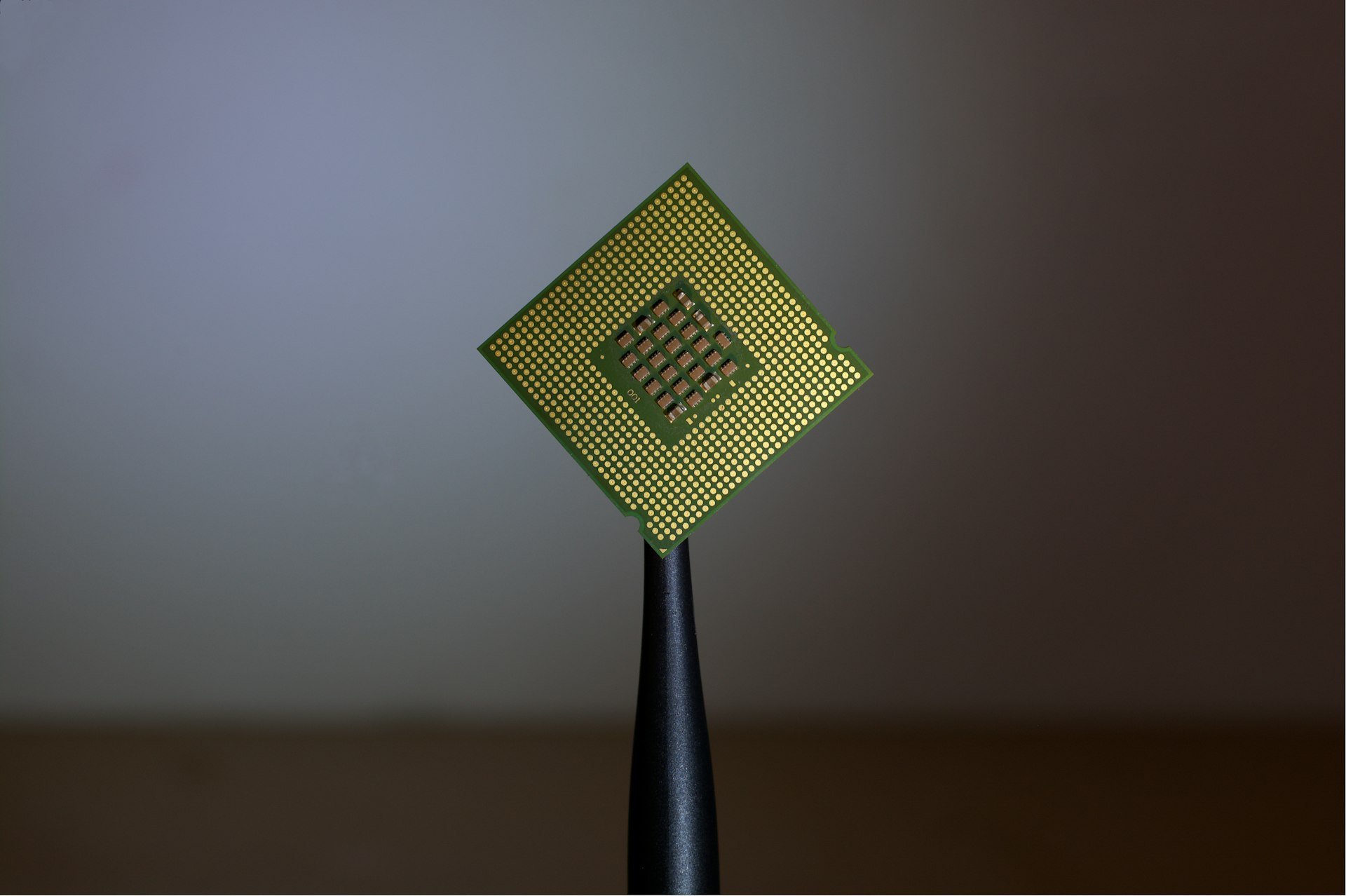
Traditional chip packaging involved mounting a single die onto a substrate, connecting it to external pins, and encasing it in plastic. While effective for many years, this approach struggled to keep up with the demand for more compact, high-performance devices. Advanced packaging techniques address these limitations by rethinking how chips are arranged and interconnected, allowing for closer integration of multiple components. This shift has not only extended the lifespan of Moore’s Law but also opened up new avenues for innovation that were previously unavailable with traditional manufacturing methods.
One of the most impactful advanced packaging methods is 3D stacking, which involves stacking multiple dies vertically and connecting them through tiny vias (vertical interconnect access). This approach reduces the distance between components, cutting down on signal latency and power usage. For example, memory chips can be stacked directly on top of a processor, enabling faster data transfer than if they were placed side by side on a motherboard. Companies like Intel and Samsung have invested heavily in 3D stacking technologies, with products like Intel’s Lakefield processors and Samsung’s HBM (High Bandwidth Memory) modules leveraging this approach to deliver improved performance. 3D stacking also allows for the integration of different types of chips, such as logic and memory, in a single package, creating more versatile and efficient devices.
Fan-out wafer-level packaging is another key innovation that eliminates the need for a separate substrate. Instead, chips are embedded in a mold compound, and interconnects are formed directly on the wafer. This allows for smaller package sizes and better electrical performance, making it ideal for mobile devices where space is at a premium. FOWLP has gained widespread adoption in the smartphone industry, with manufacturers like Apple and Qualcomm using it to create thinner, more power-efficient chips. Unlike traditional packaging methods, FOWLP also supports higher input/output (I/O) densities, which is essential for devices that require fast data transfer rates, such as 5G-enabled smartphones and high-resolution cameras.
Chiplet technology takes advanced packaging a step further by breaking down a single large chip into smaller, specialized modules (chiplets) that are assembled together in a single package. This modular approach offers several advantages: it reduces manufacturing costs by allowing companies to produce smaller, more yield-efficient chiplets, and it enables greater flexibility in designing chips for specific applications. For instance, a processor can combine a high-performance computing chiplet with a dedicated AI accelerator chiplet, optimizing performance for both general tasks and machine learning workloads. The AMD Ryzen 7000 series processors are a prime example of chiplet design, using multiple Zen 4 core chiplets and a separate I/O chiplet to deliver exceptional performance. Chiplet design also allows for easier upgrades, as companies can swap out individual chiplets to improve specific features without redesigning the entire chip.
Despite the many benefits of advanced chip packaging, there are several challenges that must be addressed. Thermal management is a major concern, as closely packed components generate more heat that needs to be dissipated efficiently. Additionally, ensuring the reliability of interconnects between stacked or modular chips is critical, as even a single faulty connection can render an entire device useless. Researchers are exploring new materials and cooling solutions to overcome these challenges, such as using graphene for better heat conduction and developing advanced testing methods to detect defects in packaged chips. Another challenge is standardization, as different manufacturers use different packaging technologies, which can create compatibility issues for device makers.
Looking ahead, advanced chip packaging will continue to evolve, with new technologies like heterogeneous integration (combining different types of chips, such as silicon and gallium nitride) and 2.5D packaging (placing chips side by side on a silicon interposer) gaining traction. These innovations will enable the creation of even more powerful and compact devices, driving progress in fields like autonomous vehicles, quantum computing, and wearable technology. Heterogeneous integration, in particular, will allow for the combination of chips with different materials and functionalities, opening up new possibilities for devices that can perform multiple tasks with unprecedented efficiency.

As the semiconductor industry continues to push the boundaries of what’s possible, chip packaging will remain a cornerstone of innovation. By investing in these advanced techniques, companies can unlock new levels of performance and efficiency, ensuring that digital technology continues to evolve and improve the way we live and work. The future of chip packaging holds great promise, and it will be exciting to see how these innovations shape the next generation of electronic devices.
MORE FROM lowcostbotox.com